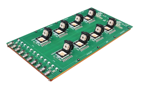
Semiconductor testing refers to product testing based on ATE machines, which is divided into wafer level CP testing (chip probing) or FE testing (FrontEnd test) and post packaging FT testing (final test) or BE testing (backend test). Of course, with the promotion of WLCSP (wafer level chip scale package) packaging, more and more products can be cut and supplied in pieces after CP testing.
Traditional semiconductor testing heavily relies on DFT design, and a complete DFT design can provide testing incentives with high fault coverage, ensuring that semiconductor testing can screen out faulty chips with minimal time cost. However, with the increasing complexity of chip software and hardware, many problems cannot or are difficult to abstract corresponding fault models. Therefore, SLT (system level test) is also adopted by most companies to ensure the fault coverage of the entire FT test after FT testing, ensuring that DPM (defects per million) meets customer needs.

1. Semiconductor testing plan
Pad related testing
Covering IO contact, Pad leakage, Pad pull up&pull-down, input-output VIX/VOX/IOX testing, and output impedance testing. The testing principle is very simple, based on Ohm's theorem for measuring current and voltage. But this type of test can effectively filter out faults related to pads/bumps/balls, which often occur in wafer cutting,
Power current related testing
Covering SICC (static/package current), DICC (dynamic work current), and sleep current. Testing can evaluate the power consumption indicators of DUT and classify products into different categories based on user requirements for power consumption. By using PAT (Part Average Testing) technology, adaptive test limits can be used to screen out chips with abnormal power consumption.

Performance related tests
Generally, core/CPU/DPS requires testing of performance related parameters such as maximum operating frequency and minimum operating voltage. These test results are used for product classification and specific settings of DVFS (Dynamic voltage and frequency scaling) during system software operation.
Scan test
The fault coverage of digital logic is mainly guaranteed by DFT's scan, and the scan coverage of most products is above 95%. The Scan test motivation is generated by EDA tools based on fault models (such as stuck at fault, transition fault, bridge fault, etc.). Compared to traditional functional stimulation testing, the advantage is that it can achieve maximum fault coverage with minimal testing time, and generally does not require high-speed testing machines. It also avoids asynchronous communication requirements between DUT and testing machines. Moreover, DUT testing failures can be traced back to specific design circuits, making it easier for later analysis. The Scan test mainly depends on the design of DFT/DFM, and requires sufficient communication during the design phase regarding coverage, fault model, vector size, pulse current during shift, and so on.
Mbist test
Sram occupies a large area in SoC, and similar to digital logic, Sram has a mature built-in self-test solution mbist to ensure 100% fault coverage. Sram also has various fault models (stuck at, transition fault, address fault, coupling fault, neighborhood sensitivity, stability fault, retention fault, etc.), and multiple mbist algorithms need to be selected based on the stability of the process and DMP requirements to ensure strong testing.
High speed digital interface testing
SoC generally integrates many digital high-speed interfaces, such as USB, MIPI, PCIE, SATA Wait a minute. The data rate of these interfaces is above 2GHz, and most ATE testing machines cannot support such high frequencies with regular PE cards. Choosing a high-speed board means a significant increase in testing costs.
Analog module testing
Covering PLL, LDO, bandgap, OSC and so on
PCBA Design Productivity Processing Services
1、 Preliminary preparation stage: Clarify the requirements of the PCBA project and prepare for project initiation
2、 Design and development: Design circuit designs that comply with SMT processing and production processes
3、 Trial production meeting held: issues to be noted during production, optimization of pre production processes
4、 Production process operation manual: The production operation manual is consistent with the PCBA processing plant
5、 Confirmation of Steel Mesh Manufacturing Capability: Produce suitable steel mesh according to gerber documents
6、 Tile mounting machine: programming and mounting according to BOM list, measuring PCB size and splicing processing
7、 PCBA testing: appearance, aging, burning, high and low temperature, ICT testing
8、 PCBA SMT project evaluation: PCBA design mutual inspection, process improvement, etc
By doing the above eight steps well, the PCBA plan will continue to improve. Further optimize PCBA design to enhance product manufacturability and lifecycle.